Understanding the Technical Challenges in the Solar Panel Silicon Value Chain
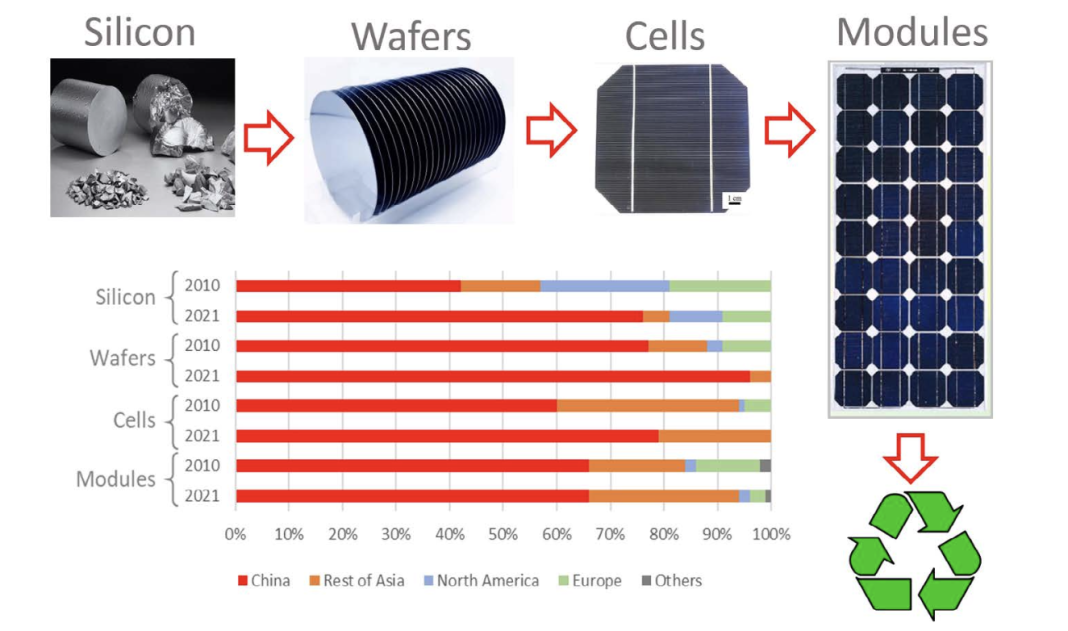
The silicon value chain lies at the heart of the global solar panel industry. From the transformation of raw quartz sand into ultra-pure polysilicon, to the assembly of advanced solar modules, each stage of the process is highly technical and resource-intensive. While solar energy represents a clean and renewable alternative to fossil fuels, the path from raw materials to finished modules is filled with engineering, economic, and environmental challenges.
This article explores the key technical challenges that impact the silicon value chain and discusses how the industry is responding with innovation, efficiency improvements, and sustainable practices.
1. Polysilicon Production: Energy and Purity
Polysilicon is the foundation of photovoltaic technology, but producing it is extremely energy-intensive.
- Challenge: Traditional Siemens-based purification requires temperatures above 1,000°C and consumes vast amounts of electricity.
- Purity Requirements: Solar-grade polysilicon must reach 99.9999999% purity (9N). Even tiny impurities can drastically reduce efficiency.
- Industry Response: Fluidized Bed Reactor (FBR) technology is emerging as a lower-energy alternative, while renewable-powered production facilities aim to reduce carbon emissions.
2. Ingot Growth: Crystal Perfection vs. Production Cost
Once polysilicon is purified, it is melted and re-crystallized into ingots. Achieving defect-free crystals is a technical hurdle.
- Monocrystalline Ingots: Offer higher efficiency but require precise growth control, making them costly and slow to produce.
- Multicrystalline Ingots: More affordable but suffer from grain boundaries that reduce electron mobility.
- Main Challenge: Balancing cost, speed, and crystal quality.
3. Wafer Slicing: Material Loss and Fragility
Slicing ingots into wafers is a delicate process with two main challenges:
- Kerf Loss: Up to 40% of silicon is lost as fine dust during traditional wire sawing.
- Fragility: Thinner wafers improve efficiency but increase breakage during handling.
- Solutions: Diamond wire cutting reduces waste, while advanced automation minimizes wafer breakage.
4. Solar Cell Manufacturing: Efficiency and Stability
Transforming wafers into solar cells involves complex semiconductor engineering.
- Challenge 1: Efficiency Limits
Commercial cells average 22–25% efficiency, but theoretical limits and manufacturing tolerances keep pushing innovation. - Challenge 2: Degradation
Solar cells lose 0.3–0.5% efficiency per year due to light-induced degradation (LID) and potential-induced degradation (PID). - Challenge 3: Advanced Technologies
PERC, TOPCon, and HJT require new equipment and higher manufacturing costs. Scaling these technologies remains difficult.
5. Module Assembly: Durability and Reliability
Solar modules must endure decades of operation under harsh conditions.
- Mechanical Stress: Wind, snow, and thermal cycling can cause micro-cracks.
- Moisture and UV: Encapsulation must protect cells for 25–30 years.
- Scaling Challenge: Ensuring consistent quality in mass production while keeping costs competitive.
6. Supply Chain Bottlenecks and Geopolitical Risks
The silicon value chain is geographically concentrated, creating vulnerabilities.
- Challenge: Over 70% of global polysilicon supply comes from a few regions in China.
- Risk: Trade restrictions, tariffs, or political instability can disrupt supply and raise prices.
- Solution: Diversification of supply chains and regional manufacturing hubs.
7. Environmental and Sustainability Challenges
The environmental footprint of the silicon value chain cannot be ignored.
- High Energy Use: Especially in polysilicon production.
- Chemical Waste: Hydrochloric acid and other chemicals require careful management.
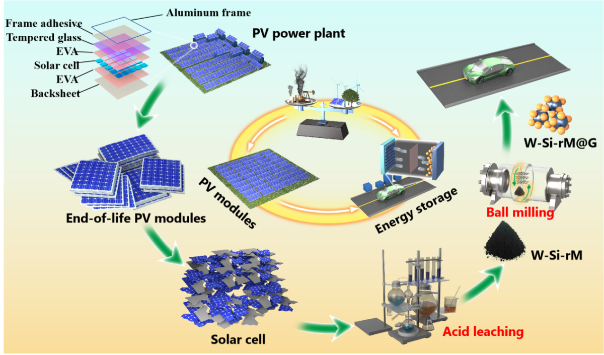
- End-of-Life Panels: Recycling infrastructure for old solar modules is still under development.
8. The Path Forward: Innovation and Collaboration
Addressing these technical challenges requires industry-wide innovation:
- R&D Investments: To improve wafer cutting, high-efficiency cell designs, and advanced encapsulation.
- Automation & AI: To enhance quality control and reduce defect rates.
- Global Cooperation: To secure supply chains and promote sustainable practices.
Conclusion
The silicon value chain is the backbone of the solar panel industry, but it is far from simple. Each stage — from polysilicon refinement to module assembly — presents unique technical challenges that shape cost, efficiency, and environmental impact.
At Han Solar Tech, we believe that facing these challenges head-on is not only necessary but also an opportunity. Through innovation, sustainability, and vertical integration, the solar industry can overcome barriers and continue driving the global transition toward clean, renewable energy.